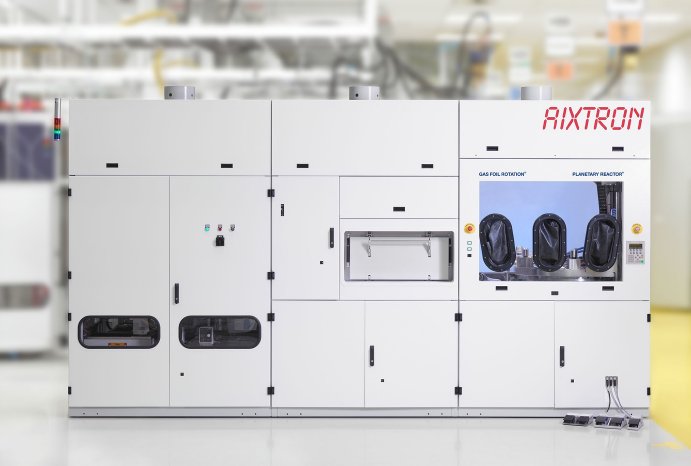
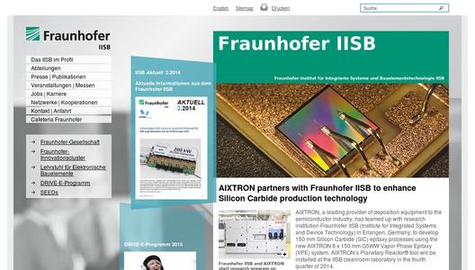
Dr. Jochen Friedrich, Head of Department Materials at Fraunhofer IISB, comments "Through this partnership we expect to further accelerate the implementation of 150 mm SiC technology in the industry by pairing our process know-how in manufacturing SiC epitaxial layers with AIXTRON's SiC equipment expertise. We will use the G5WW production system for process optimization and demonstration purposes at the IISB facilities in Erlangen."
Fraunhofer IISB has developed fundamental understanding in low-defect-density SiC epitaxial processes which are elementary for the manufacturing of high voltage SiC devices. Special characterization techniques like room temperature photoluminescence imaging and selective defect etching have been developed and adapted to the SiC material properties at Fraunhofer IISB. In its laboratories complete SiC prototype devices can be processed and characterized.
Dr. Frank Wischmeyer, Vice President Power Electronics at AIXTRON, states "Based on the worldwide recognized experience of Fraunhofer IISB in SiC epitaxy technology and characterization, we will jointly enable the optimization of epitaxial production processes for 150 mm SiC wafers using our state-of-the-art G5WW production tool. The goal of the collaboration is the demonstration of high-volume manufacturing processes addressing the SiC material requirements of SiC power devices. With this joined effort we do support AIXTRON customers worldwide moving from 100 mm to 150 mm SiC processing technology from the year 2015 to achieve efficient and economic manufacturing processes for future SiC power devices."
Today, a variety of SiC devices like Schottky Diodes and Metal-Oxide-Semiconductor Field-Effect Transistors (MOSFETs) are commercially available and put into practical use in switch mode power supplies for computer servers and TVs, in solar power inverters and efficient power converters in UPS, medical equipment or commuter trains. In order to facilitate a widespread adoption of SiC in power electronics cost reductions in SiC semiconductor material manufacturing and device processing are targeted by the implementation of the 150 mm SiC technology.
About AIXTRON:
AIXTRON SE is a leading provider of deposition equipment to the semiconductor industry. The Company was founded in 1983 and is headquartered in Herzogenrath (near Aachen), Germany, with subsidiaries and sales offices in Asia, United States and in Europe. AIXTRON's technology solutions are used by a diverse range of customers worldwide to build advanced components for electronic and opto-electronic applications based on compound, silicon, or organic semiconductor materials. Such components are used in a broad range of innovative applications, technologies and industries. These include LED applications, display technologies, data storage, data transmission, energy management and conversion, communication, signalling and lighting as well as a range of other leading-edge technologies.
For further information on AIXTRON (FSE: AIXA, ISIN DE000A0WMPJ6; NASDAQ: AIXG, ISIN US0096061041) please visit the website at: http://www.aixtron.comaixtron.com" target="_blank">www.http://www.aixtron.comaixtron.com.

