Contact
QR code for the current URL

Story Box-ID: 687488

Fraunhofer-Institut für Integrierte Systeme und Bauelementetechnologie IISB Schottkystraße 10 91058 Erlangen, Germany http://www.iisb.fraunhofer.de
Contact Mr Dr. Jochen Friedrich +49 9131 761270

Improved quality control of silicon carbide epiwafers by a new fast and contactless inline inspection tool

(PresseBox) (Erlangen, )
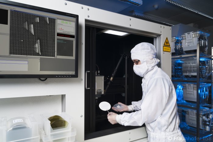
A new fast and contactless Defect Luminescence Scanner (DLS) for photoluminescence imaging of 4H-SiC epiwafers was developed under coordination of Fraunhofer IISB together with Intego GmbH. This DLS system enables a more efficient optimization of the production process of SiC epiwafers as well as an inline quality control along the device production chain. This will contribute to cost reduction in material and device production, and helps accelerating the further commercialization of SiC power devices.

With respect to structural defects, such as micropipes or other dislocation types, and their densities in substrates and epilayers, the material quality of silicon carbide (4H-SiC) has been improved greatly within the last years. But still, the performance of especially SiC bipolar devices and the yield of device production may be limited by residual structural defects in the epiwafers. Such defects originate in the substrate material or are generated during the epitaxial process like, e.g. down-fall particles, stacking faults, and dislocations.

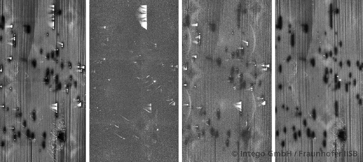
To date, several characterization methods are well established for identification and distribution of such defects on the wafer level, but they are destructive (defect selective etching), cost-intensive (synchrotron x-ray topography), or time-consuming (both defect selective etching and x-ray topography). Hence, they are not suitable for a fast inline quality control of the material preparation and device production. As a non-destructive, contactless method allowing for identification of structural defects of 4H-SiC at room temperature, the photoluminescence (PL) technique is well known. In PL images, structural defects appear either as bright or dark items on the "grey" SiC background as 4H-SiC itself shows a low PL intensity due to its indirect band gap.

However, so far no PL setup exists which is fast enough for an inline defect analysis on full waferscale within a production environment. This obstacle has now been overcome in the course of the "SiC-WinS" project, funded by the Bavarian Research Foundation (BFS) under contract number AZ-1028-12. Together with the metrology specialist Intego Vision Systeme GmbH, the new PL imaging tool called defect luminescence scanner (DLS) was designed and fabricated under coordination of Fraunhofer IISB. The DLS allows for short PL measurement cycles and high throughput of SiC epiwafers at a high lateral resolution of 5 µm.

The DLS system is installed at Fraunhofer IISB and consists of a UV laser operating at 325 nm wavelength for PL excitation, a sample stage for scanning the SiC epiwafer, and an electron multiplying charge-coupled device (EMCCD) camera for fast image recording at a high signal-to-noise ratio. The high lateral resolution of 5 µm is achieved by a magnifying objective lens in front of the camera. For identification of defect types by their spectral fingerprints, different band-pass filters are installed. The DLS system can determine the defect types and their distribution on SiC epiwafers up to 150 mm diameter in less than 30 minutes. A routine for automated defect identification and counting in order to predict directly the device yield per epiwafer is currently under development.

Fraunhofer IISB performs service measurements with the new DLS system and identifies the defects and their distribution on SiC epiwafers on the full waferscale for epi houses and device manufacturers.
Website Promotion

Website Promotion
Homepage Fraunhofer IISB

Fraunhofer-Institut für Integrierte Systeme und Bauelementetechnologie IISB

Custom-tailored SiC Services at Fraunhofer IISB:

Fraunhofer IISB offers R&D services in SiC from materials development and prototype devices to module assembly and mechatronic systems. Based on our toolbox, customers can utilize the services in order to perform, e.g., design studies, feasibility tests, proofs of concept, or prototype fabrication. Fraunhofer IISB offers competent partnership for contract research and development in bilateral cooperation with industry as well as in public-funded projects.

Fraunhofer IISB in Profile:

The Fraunhofer Institute for Integrated Systems and Device Technology IISB is one of the 67 institutes of the Fraunhofer-Gesellschaft. It conducts applied research and development in the fields of power electronics, mechatronics, micro and nanoelectronics. A staff of 200 works in contract research for industry and public authorities.

The institute is internationally acknowledged for its work on power electronic systems for energy effi-ciency, hybrid and electric cars and the development of technology, equipment, and materials for nanoelectronics.

In addition to its headquarters in Erlangen, the IISB has branch labs in Nuremberg and Freiberg.

The institute closely cooperates with the Chair of Electron Devices of the Friedrich-Alexander-Universität Erlangen-Nürnberg (FAU).

The publisher indicated in each case (see company info by clicking on image/title or company info in the right-hand column) is solely responsible for the stories above, the event or job offer shown and for the image and audio material displayed. As a rule, the publisher is also the author of the texts and the attached image, audio and information material. The use of information published here is generally free of charge for personal information and editorial processing. Please clarify any copyright issues with the stated publisher before further use. In case of publication, please send a specimen copy to service@pressebox.de.
Important note:

Systematic data storage as well as the use of even parts of this database are only permitted with the written consent of unn | UNITED NEWS NETWORK GmbH.

unn | UNITED NEWS NETWORK GmbH 2002–2024, All rights reserved

The publisher indicated in each case (see company info by clicking on image/title or company info in the right-hand column) is solely responsible for the stories above, the event or job offer shown and for the image and audio material displayed. As a rule, the publisher is also the author of the texts and the attached image, audio and information material. The use of information published here is generally free of charge for personal information and editorial processing. Please clarify any copyright issues with the stated publisher before further use. In case of publication, please send a specimen copy to service@pressebox.de.