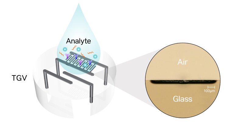
Glass is winning more and more favor as a substrate for electrical circuits. This is due to its special material properties: It maintains its dimensions over a vast range of temperatures, it is available even in large formats (e.g. full-format 24x18 inch panels), and it offers high electrical resistance, a smooth surface, and a high dielectric constant (e.g. 5.0 at 77 GHz). These properties have motivated developers for some time already to construct electrical structures like conductors as thin metal layers on and through glass substrates. Contacts can be created not just on a single layer, but also through several layers of the finished design by way of Through-Glass Vias (TGV).
Researchers at Fraunhofer IZM have developed a novel means for integrating metal conductors in glass. The highlight: The technique keeps the smooth surface of the glass intact, and it avoids any issues with the bond between the glass and the metal layer, which is fully embedded in the glass itself. No additional bonding agent – typically another metal – is needed.
The researchers managed to develop a process for controlling the formation of metal structures in thin glass. In their effort to create homogeneous electrical conductors near to the glass surface, they tested a range of materials and processing techniques to find the best possible approach. The key to their success lies in both the choice of material and the new processing technique: The metal layer can be extremely thin, down to several hundred nanometers, or visible to the naked eye at micrometer thickness due to the strong reflection creating a mirrorlike effect on the glass surface. The technique can create metal layers with lengths ranging from several millimeters up to ten centimeters, and it is versatile enough to integrate very specific metal structures and create electrical conductors within the glass itself.
“Electrical signals can now be routed through the conductors without worrying about environmental factors like aggressive liquids, gases, chemical reactions like corrosion, or simple mechanical wear and tear. The structures are completely enclosed by the glass and not simply placed on top of it”, says Philipp Wachholz, research assistant in the EOCB team (electrooptical circuit boards).
The new ability to embed electrical conductors inside and not on glass opens the doors for many novel applications. It would be possible to fit glass micro vacuum chambers with electrical contacts, without compromising their hermetic seal. Glass-integrated conductors could also be used in adverse conditions that surface-mounted conductors would not withstand, e.g. for rugged sensors. Tiny microelectrodes could be used for electrochemical biosensors to record biochemical processes like enzyme reactions or antigen antibody interactions. With the glass-integrated structures easily coping with temperatures up to 200°C, the possibilities for extremely robust sensors seem limitless.
And the researchers at Fraunhofer IZM are ready to test these limits: After successful feasibility studies, they want to team up with partners from science and industry to bring the new technology to active use. For this purpose, they are currently looking for and waiting to hear from interested industry partners to share in their glass expertise.
Benefits of glass-integrated electrical metal structures over surface vapor deposition:
- No bonding issues on the glass surface
- Electrically conductive microstructures embedded in glass: electrical vias
- Integration of other electrical structures possible (resistance, capacitors etc.)
- Metal structures safe from environmental forces:
- Corrosion-proof
- Protected against wear and tear
- Glass surfaces easily cleaned
- Glass conducts heat away from the metal microstructures
- Reduced CTE difference between metal and glass structures


