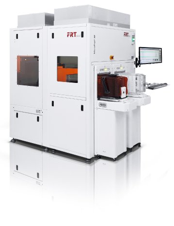
The MicroProf® AP is ideally suited to perform measurement tasks of typical process steps in advanced packaging, like
- photoresist coating and structuring,
- Critical dimension (CD) and overlay
- measurement through-silicon vias (TSVs) or trenches after etching,
- isolation and barrier layer deposition,
- TSV filling,
- chemical mechanical polishing (CMP),
- fabrication of redistribution layers (RDLs), under bump metallization (UBM), BGAs, micro and solder bumps,
- temporary carrier bonding and debonding,
- backside thinning,
- reveal of TSV copper nails,dicing and stacking and
- measurement of mold- and contact pad surfaces.
The measurement system of the MicroProf® AP is equipped with a granite base setup, with a three point sample fixture or a vacuum chuck. Besides the standard configuration, the tool can be equipped with numerous additional features, which can also be retrofit at a later time.
With a wafer handling system within an Equipment Front End Module (EFEM) and almost maintenance free hardware components, the MicroProf® AP provides high throughput and is the perfect workhorse in any HVM 3D IC fab.
The newest member of our MicroProf® family is born! FRT GmbH will present more detailed information at Semicon Europa, hall A4, booth 411!


