Acquiring and integrating the processing-machining data from this laser system will allow a useful database to be built for optimizing laser processing conditions by using artificial intelligence (AI). This will not only streamline laser processing-machining tasks but also open up new frontiers in energy and medical and applications.
Hamamatsu Photonics plans to announce this achievement at the NEDO booth during the OPIE ’21 (OPTICS & PHOTONICS International Exhibition 2021). This is Japan’s largest optoelectronics exhibition and will be held at the Pacifico Yokohama (Nishi-ku, Yokohama, Japan) from Wednesday June 30th through to Friday July 2nd 2021. Laser-machining samples will also be on exhibit.
1. Overview
At future manufacturing sites, production equipment will be linked through cloud computing to streamline automation and enable labor-saving by using AI and harnessing the IoT (Internet of Things) that connects everything via the internet. These types of high-tech innovations are making lasers an essential tool for future manufacturing because laser machining and processing conditions are easy to control digitally.
Lasers used for material processing and machining are broadly classified into two groups. One group is CW (continuous wave) lasers that continuously emit light at a constant intensity. The other group is pulsed lasers that repetitively emit pulsed light at very short time intervals. CW lasers are used for heat treatment tasks such as laser welding and cutting making them the mainstream tool for laser processing and machining. Pulsed lasers, on the other hand, have not yet been widely used in these applications except for laser peening*1). This is because high-power semiconductor lasers (laser diodes, or LD) and large-size laser mediums that are needed for developing high-power pulsed laser systems have not been available. This has hindered the task of setting up systems to find critical processing and machining conditions such as the optimum irradiation time and energy.
To overcome these challenges, Hamamatsu Photonics have been developing high-power pulsed laser systems as part of the “Development of Advanced Laser Processing with Intelligence Based on High-Brightness and High-Efficiency Next-Generation Laser Technologies (TACMI Project)” *2) supported by the New Energy and Industrial Technology Development Organization (NEDO), which is a national research and development agency in Japan. In 2019, we developed an industrial pulsed laser*3) that produces a pulse energy of 117 joules by using 4 LD modules*4 that we manufactured in-house and 2 laser amplifiers*5) each equipped with 6 ceramic laser mediums *6).
We continued efforts to further boost the output power and this time succeeded in creating an industrial pulsed laser system that delivers a pulse energy of 250 joules, which is the world’s highest energy among LD-pumped lasers*7). At the same time, using this new laser system, we also evaluated basic conditions essential for designing a 1 kJ (kilojoule) class laser, which will prove an important milestone in laser technology development, and confirmed that it is practical and achievable.
Hamamatsu Photonics plans to announce this achievement at the NEDO booth of the OPIE ’21*8). This is Japan’s largest optoelectronics exhibition and will be held at the Pacifico Yokohama from Wednesday June 30th through to Friday July 2nd 2021. We will also exhibit laser-machined samples.
2. Our current results
[1] Industrial pulsed laser system that produces an output of 250 joules which is the world’s highest level among LD-pumped lasers
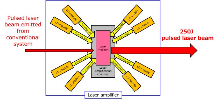
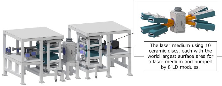
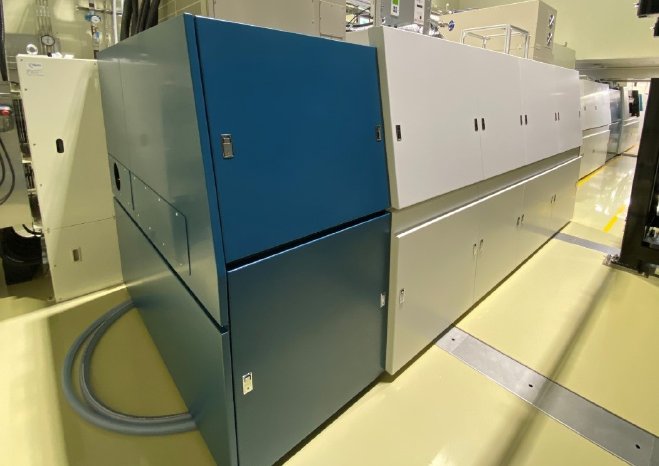
Compared to our previous system, this new laser system has approximately double the light energy storage capacity. We achieved this by installing a laser medium composed of 10 ceramic disks, each with the world largest surface area optimized for a laser medium. We also reassessed and revamped the amplifier design and utilized 8 of our newly designed compact LD modules mounted at ideal irradiation angles and positions. Doing this increased the pumping efficiency to the laser medium and improved the pumping capacity to about twice that of the previous system (see Fig. 1 and Fig. 2). What’s more, we have achieved high beam quality that gives them good light focusing properties and a highly uniform output distribution on the irradiated surface by optimizing the optical design of the entire system via our unique high-power laser technology. This allowed our new laser system to deliver a high power of 250 joules that more than doubles the energy amplification capacity, achieving the world’s highest pulse energy among LD-pumped lasers. Yet even with such high power it is still just about the same size as currently available industrial pulsed lasers (see Fig. 3 and Table 1).
Acquiring and integrating the processing-machining data obtained with this new laser system will allow us to build up a useful database and to optimize the processing conditions using AI. This will help streamline laser processing-machining tasks.
[2] Confirmed the feasibility of fabricating an industrial pulsed laser with 1 kJ output
Using this new pulsed laser system, we evaluated the basic conditions necessary for designing a 1 kJ class laser which will prove an important milestone in laser technology development. As a result, we confirmed that fabricating a 1kJ class laser is practical and achievable by quadrupling the beam size while maintaining current performance. If we can fabricate a 1 kJ class laser, it will extend laser applications into new fields such as medicine, energy, new materials and basic science in addition to spearheading new laser processing-machining technology.
3. Future approaches
In cooperation with the TACMI Consortium*9), Hamamatsu Photonics and NEDO will proceed with building up a database that integrates laser processing-machining experiments and data acquired from using this new laser system. Hamamatsu Photonics will also continue research work aiming at making the 1kJ industrial pulsed laser system a reality.
[NOTES]
*1: Laser peening
A metal surface hardening process utilizing shock waves generated by instantaneous irradiation of high energy
*2: Development of Advanced Laser Processing with Intelligence Based on High-Brightness and High-Efficiency Next-Generation Laser Technologies (TACMI Project)
This project aims to develop new laser technologies that deliver unprecedentedly high luminance (high output power and high beam quality) and high efficiency. It has the further goal of developing innovative laser processing technology using new laser technologies that will lead the rest of the world in accelerating its universal spread to manufacturing sites. This project has encompassed a total of five challenging R&D themes from 2016 through 2021. Our newly developed pulsed laser is the result of work on “Development of new processing technology using high-energy pulse lasers” which is one of those five themes.
*3: Development of industrial pulsed laser that produces a pulse energy of 117 joules
News release from Hamamatsu Photonics: “Hamamatsu Photonics has developed a laser-diode-pumped industrial high-energy pulsed laser system that delivers the world’s highest output of 117 joules” (April, 2019).
https://www.hamamatsu.com/...
*4: LD module
A light source consisting of multiple semiconductor lasers, optical components, power supplies, etc.
*5: Laser amplifier
A device consisting of semiconductor laser modules and a laser medium that can amplify the input laser energy and output the amplified energy.
*6: Laser medium
A material that stores energy from an external source and imparts that energy to the laser light passing through it to amplify the optical power.
*7: Pumping
Process in which atoms and molecules are excited to a higher energy level by absorbing light.
*8: OPIE ’21
A technology exhibition that brings together the latest technologies, products, and information about light and lasers.
Name: OPIE’21 (OPTICS & PHOTONICS International Exhibition 2021)
Date: Wed. 30 June – Fri. 2 July 2021 (10:00 – 17:00)
Place: Pacifico Yokohama, 1-1-1 Minato Mirai, Nishi-ku, Yokohama 220-0012, Japan
For more information: NEDO Website (Events page)
(https://www.nedo.go.jp/...)
*9: TACMI Consortium
TACMI Consortium: Consortium for “Technological Approaches toward Cool laser Manufacturing with Intelligence” established and managed mainly by the University of Tokyo for the purpose of making laser processing platform and tools provided by NEDO project implementers widely available to the industry and promoting new manufacturing using lasers to meet the needs of the era of IoT.
For further information contact us on email: europe@hamamatsu.de or visit our website: www.hamamatsu.com


