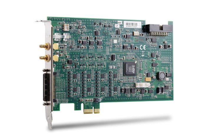
The PCIe-7350 offers 32 channels of bi-directional parallel I/O lines with a data throughput of up to 200 MB/s and a clock rate up to 100 MHz.
The PCIe-7350 offers a low-cost, high-throughput architecture with very flexible acquisition/generation timing and triggering features-making it an ideal solution for high-speed digital pattern acquisition and generation for use in ATE, IC testing, image sensor testing, and video image recording/playback. The PCIe-7350 is based on the PCI Express® interface (x1 lane), supports a selectable input/output direction per group of eight bits, and provides eight channels auxiliary programmable I/O. An onboard FPGA provides addition I/O features such as triggers, clock signals, handshaking lines, and I2C and SPI control interfaces. These on-board interfaces enable the PCIe-7350 to communicate with external image sensors via I2C and SPI, without the need for a external control interfaces.
"As the resolution of image sensor increases, the image data throughput and higher pixel clock rate support of current solutions are becoming insufficient. A high-speed DIO card with flexible timing and trigger modes is now the ideal solution," stated James Gau, vice president of the measurement and automation product segment at ADLINK Technology. "ADLINK's PCIe-7350 provides higher throughout and clock rates to increase testing speeds and thus lowers costs; its data throughput through the x1 PCI Express bus interface is sufficient for capturing high resolution image patterns at a high frame rate, which makes it an ideal solution today for image sensor testing."
The PCIe-7350 supports selectable software voltage levels of 1.8, 2.5, and 3.3 V (5 V compatible) which provides the flexibility of interfacing with a variety of ASICs or external devices. The PCIe-7350 also supports a 16-step phase shift feature to ensure accurate sampling timing and prevent invalid timing issues during data transition.
Please visit www.adlinktech.com/MAPS/ for more information.

