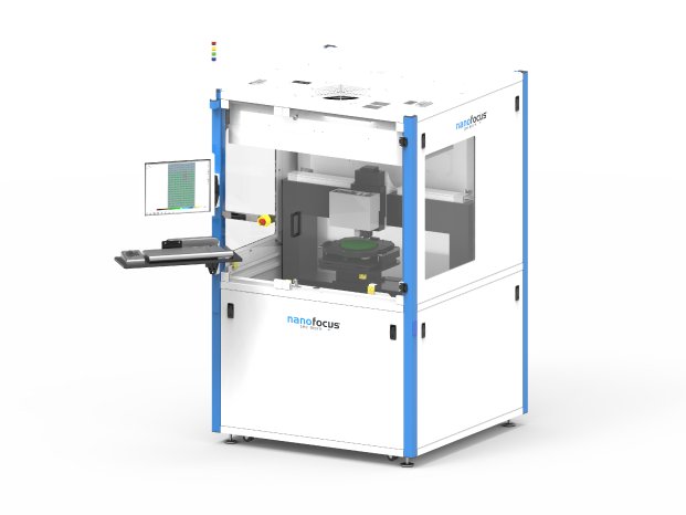
µsprint hp-opc 3000 is applied for the inspection of probe cards, which are special test devices used for standard function tests of wafers. Since wafer testing can only take place after the functional structures on a wafer are fully manufactured, damage of wafers during testing represents a significant economic loss.
At this point, the inspection system µsprint hp-opc 3000 enables a novel and innovative process step. The measuring system ensures that the wafers are in sound condition after testing. It consequently contributes to reducing operational costs, minimizing yield losses as well as increasing quality in wafer production.
„We are pleased about the positive feedback of industry experts. It proves that µsprint hp-opc 3000 is a tailor-made solution to current requirements and expectations of wafer manufacturers,” says Martin Kunz, Head of Business Unit Semiconductor at NanoFocus. The potential and advantages of the tool were recognized in particular for wafer test locations with large-volume throughput and for the manufacturing process of probe cards. Additionally, the compatibility to existing probe card testing processes was positively received.
A pilot system already is successfully installed at a renowned manufacturer of semiconductor elements. Further orders are expected in the third quarter 2016.


