The STM32F7 series MCUs not only feature a Cortex-M7 core that can be operated at frequencies up to 216 MHz, but also up to 1 Mbyte embedded Flash, 320 Kbytes SRAM and high-performance peripheral units (graphic accelerator, Ethernet, USB and audio interfaces, etc.).
As is usual with PLS, the UDE 4.5 also fully supports all on-chip peripheral units and internal debug functions. This also applies to the Floating Point Unit (FPU) integrated in the Cortex-M7. The debugger takes over, for example, display of the respective instructions and additional registers. Even the code and data cache ‒ provided for the first time in a Cortex-M architecture ‒ which permits program execution with 0-wait-state performance from both the on-chip Flash and the external memory, is fully taken into account by the debugger during control of the target and display of the memory.
The real-time characteristics of the STM32F7 family benefit, among other things, from the many possibilities of the graphical representation of system parameters within the UDE 4.5 and the comprehensive support of the integrated units for program, data and performance traces.
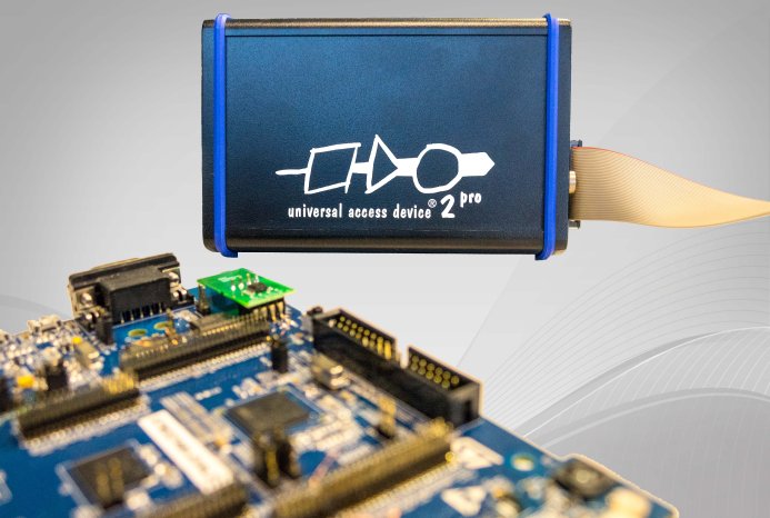
Connection to the target is optionally possible via JTAG or via the more modern Serial Wire Debug (SWD) interface. A digitally isolated connection between the target and the Universal Access Device (UAD) is also possible if required. The programming function integrated in the UDE 4.5 ensures maximum speeds when erasing, programming and verifying the on-chip Flash memory. Furthermore, in combination with PLS’ Universal Access Device 2 (UAD2) family, developers can use the built-in Bootstrap Loader (BSL) implemented in the STMicroelectronics STM32F7 series of MCUs to optionally program the on-chip Flash memory via an asynchronous serial interface or the CAN bus.
The complete cross-debugger functionality of the UDE 4.5 is also available fully integrated in Eclipse via an own debug perspective.


