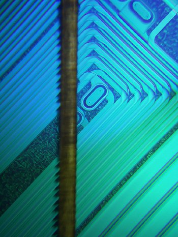
The processes involved in manufacturing thin films have much in common with the production of semiconductors, so they are understood well enough. However, there is still a huge amount of untapped potential in thin-film technology. The reason this potential has yet to be realised is not simply lack of knowledge of other areas of application, but also the great cost and development levels associated with the production facilities.
In terms of other applications outside the semiconductor manufacturing sector, sensor technology comes to mind first and foremost. Thin films react sensitively and reproducibly when exposed to force, deformation, temperature, light, chemical substances, etc. With the appropriate design they can also detect magnetic fields and electrical flows with a spatial resolution of just a few µm.
Nickel, chrome, copper, SiO2, TiON and NiCr are just some of the materials that can be applied to any smooth surface in films of up to 1.5µm with outstanding adhesion. Structuring is possible from a width of 10µm. One option for TFT that has hardly been utilised yet is direct application onto specific deformation elements. Films applied to 50µm-thin sheets of metal, for example, have already enabled a brand-new magnetic positioning technique.
The successful application of TFT requires expert analysis of the project's suitability. The strengths of the technology must be defined and known: Extremely versatile and multi-layer application of a variety of materials, marginal spatial requirements, low unit costs, high stability and robustness (up to 300°C), precision measurements that can be reproduced, extremely high adhesion - these advantages open up a wide spectrum of applications.
However, the technology's weaknesses, such as high initial costs, complex development and production processes, limited geometries when it comes to substrates, limited choice of materials and challenging bonding techniques, also have to be discussed between users and TFT experts.
If TFT provides an elegant solution to a particular problem, initial concepts must be prepared and assessed with the customer and a cost/benefit analysis carried out. The decision centres on whether a four-figure investment (EUR) should be made in order to create prototypes of the preferred design. There is still a long way to go before the first parts go into series manufacture and are supplied to the customer. Sensor-Technik Wiedemann (STW) can offer these services when required: Simulation, product and process design, sample production, verification and subsequent initiation of series manufacture in accordance with the ISO/TS 16949 standard.
STW, based in Kaufbeuren, Germany, has acted as a key TFT partner in a number of successful projects and is now expanding its range of services accordingly. The target group for this new service area comprises companies that are looking to take advantage of the potential of TFT but that do not have access to the necessary expertise or production facilities themselves.
As a TFT service provider, Sensor-Technik Wiedemann will be opening up its expertise on the technology and in-house production facilities to other companies moving forward.
As a result, users will have the opportunity to use TFT in their own products - and be accompanied by experts every step of the way, from the concept right through to series manufacture.


