Serial NOR Flash also offers this kind of functionality, but requires a rather dedicated semiconductor process technology using up more chip real estate and is therefore not as competitive in write-performance, power-consumption and bottom line cost-effectiveness as serial NAND Flash of comparable memory size, that in turn enables larger memory subsystems.
Zentel, originally a DRAM specialist, uses its mother company Powerchip Technology Corp. as exclusive wafer fab also for the floating gate process technology of non-volatile NAND Flash. This single-level cell (SLC) technology is different from the usual multi-level cell (MLC) approach as used in commercial USB memory sticks or SD memory cards which only allows for a few thousand erase cycles. The 40nm-SLC technology is far more robust and hence used for solid state drives (SSD) in enterprise-class servers, where a minimum endurance of one hundred thousand re-write cycles is mandatory.
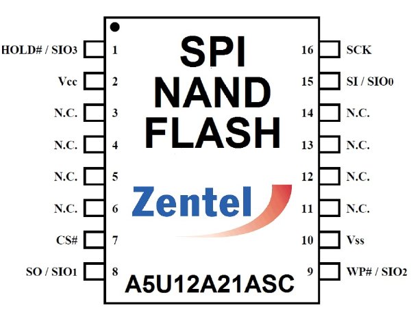
The new A5U12A21ASC compact serial 512Mbit memory chip is encapsulated in a SOP16 package with 10.5 x 10.5mm footprint - close to the less cost-effective standard 9 x 11mm VFBGA63 package size but with a relaxed 1.27 mm lead pitch compared to a more assembly-challenging 0.8 mm ball pitch.
The A5U12A21ASC provides integrated error correction as well as wear level mapping functionality.
It reserves 60 kilobytes of only one-time-programmable memory space for manipulationsafe storage of sensitive data such as device type or serial numbers and other identification or branding code as well as authenticatable server addresses for remote firmware maintenance routines. This way it also enables support of future business models such as pay-per-use in an emerging Internet-of-Things era.


