Nitride semiconductors are a strong research focus worldwide, since wide band gap semi-conductors such as GaN and AlN have turned out to be the best choice for power electronic and optoelectronic devices with enhanced power efficiency or optical performance. GaN LEDs are increasingly dominating global lighting, and electronic GaN devices are expected to achieve a substantial volume in the market soon. However, one of the key requirements for boosting the market share of nitride devices and helping to develop green technologies is the availability of cheap, high quality native substrates, which is expected to have a great impact on the further development of power electronic systems for high power applications and high brightness LEDs and high power laser diodes.
Fraunhofer IISB has more than a decade of experience in the field of bulk nitride semi-conductors and is currently doing research on the HVPE growth of GaN crystals and on the growth of nitrides with the ammonothermal technique. The latter project is in close collaboration with the University of Erlangen - Nuremberg within the "Ammonothermalsynthesis" research group funded by the German Science Foundation DFG. Part of the research of Fraunhofer IISB additionally focuses on the correlation of the electrical performance of the devices with the quality of the substrates and epitaxial layers. It was therefore a great honor that Dr. Elke Meissner from Fraunhofer IISB was selected by an international steering committee to host the 8th IWBNS workshop.
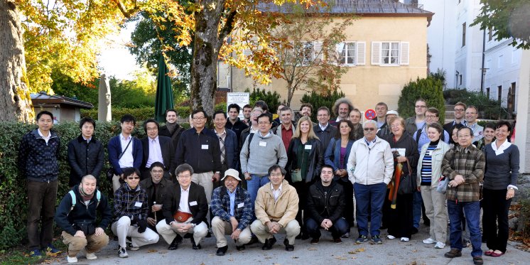
The IWBNS workshop is the only expert meeting in the world that is specially dedicated to the science and technology of the crystal growth of bulk nitrides. About the number of participants, the eighth IWBNS workshop was the largest one ever held. More than seventy renowned international experts from ten nations in Asia, the United States, South America and Europe gathered for the first time in Germany at the beautiful, scenic location of Kloster Seeon in southern Bavaria.
It was an amazing meeting with an extremely high scientific level due to the outstanding contributions of the participants. The workshop covered the crystal growth and technology of GaN, AlN, InN and other binary nitrides. "The quality of the papers was the highest of the five of these meetings I have attended," said James Edgar from Kansas State University. Jan Weyher from the Polish Academy of Science commented, "It was a very stimulating work-shop, perfectly organized."
The IWBNS has classic individual scientific spirit, intensity and character. It is designed to implement and increase an intense exchange of information that is as open as possible as well as deep scientific discussion and collaboration among academic, industrial, and government scientists regarding the challenges of growing high quality group III nitride crystals with a low concentration of structural defects and a controlled conductivity type. The very dense program of the 8th IWBNS clearly demonstrated the great necessity for further intensive exchange among experts in this field in order to further promote the penetration of the wide band gap materials into the market for energy efficient LEDs and power devices.
The organizers of the 8th IWBNS workshop gratefully acknowledge the support of several organizations that helped to make the meeting successful and the generous support for the participation of young scientists by the German Association of Crystal Growth DGKK and the International Union of Crystallography IUCR.


