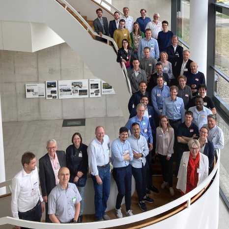
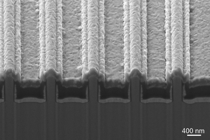
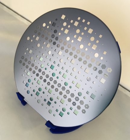
Since the project launched on May 1, 2021, impressive developments have been made by the project consortium, consisting of 23 European partners. Vertical device demonstrators with FinFET architectures and Schottky diodes – being important building blocks for a novel vertical membrane transistor technology – have been created successfully. Also, vertical layer stacks have been grown on silicon and sapphire with a diode breakdown voltage exceeding 500 V. This is a major step to reach the overall project goal of 1200 V blocking voltage on low-cost silicon or sapphire substrates. As a result, the market for future high-performance applications, e.g., in the automotive industry, could be accessible for the GaN semiconductor material.
For vertical GaN power transistors with ultra-low resistance contribution from the backside contact, the development of a reliable membrane process technology is crucial. YESvGaN has succeeded in producing such fragile GaN membranes with a thickness of a few micrometers and a diameter of several millimeters without breaking. Novel assembly and interconnection technologies are being tested for the final application of membrane vertical GaN power transistors under extreme conditions. This includes operating temperatures of more than 250 ⁰C. In addition, virtual prototypes are being developed to evaluate the efficiency of GaN devices in the target applications using digital twins.
We are confident that YESvGaN will continue to achieve promising results in the next phases of the project and take a significant step towards fully vertical GaN membrane transistors.
So, can we contribute with energy-efficient low-cost vertical GaN technology to the worldwide energy challenge? Our answer remains: YESvGaN!
This project has received funding from the ECSEL Joint Undertaking (JU) under grant agreement No 101007229. The JU receives support from the European Union’s Horizon 2020 research & innovation program and Germany, France, Belgium, Austria, Sweden, Spain, Italy.


