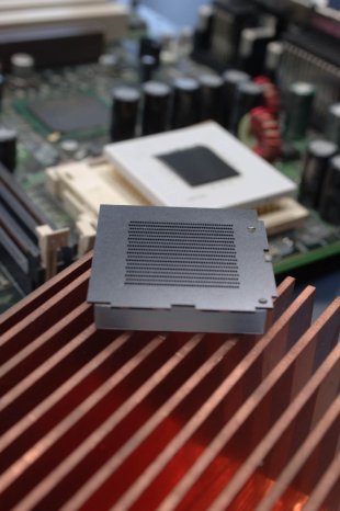
The technique, called "high thermal conductivity interface technology," allows a twofold improvement in heat removal over current methods. This paves the way for continued development of creative electronic products through the use of more powerful chips without complex and costly systems simply to cool them.
As chip performance continues to progress according to Moore’s Law, efficient chip cooling has become one of the most vexing problems for designers of electronic products. The IBM technique outlined today is one of several being explored by scientists from the IBM Zurich Research Laboratory to address the issue.
"Electronic products are capable of amazing things, largely because of the more powerful chips at their heart," said Bruno Michel, manager of the Advanced Thermal Packaging research group at IBM’s Zurich lab. "We want to help electronics makers keep the innovations coming. Our chip-cooling technology is just one tool at our disposal to help them do that."
The approach used by IBM addresses the connection point between the hot chip and the various cooling components used today to draw the heat away, including heat sinks. Special particle-filled viscous pastes are typically applied to this interface to guarantee that chips can expand and contract owing to the thermal cycling. This paste is kept as thin as possible in order to transport heat from chip to the cooling components efficiently. Yet, squeezing these pastes too thin between the cooling components and chip would damage or even crack the chip if the conventional technologies are used.
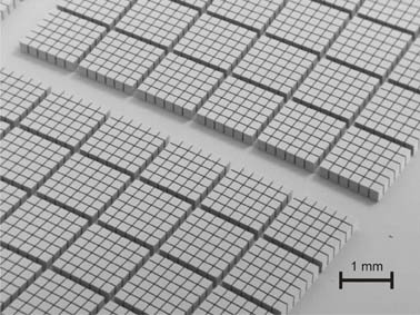
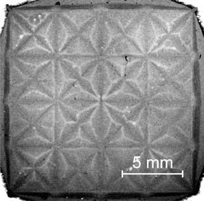
Using sophisticated micro-technology, the IBM researchers developed a chip cap with a network of tree-like branched channels on its surface. The pattern is designed such that when pressure is applied, the paste spreads much more evenly and the pressure remains uniform across the chip. This allows the right uniformity to be obtained with nearly two times less pressure, and a ten times better heat transport through the interface.
This unique and extremely powerful design for chip cooling is borrowed from biology. Systems of hierarchical channels can be found manifold in nature, e.g. tree leaves, roots, or the human circulatory system. They can serve very large volumes with little energy, which is crucial in all organisms larger than a few millimeters. Ancient water irrigation systems also used the same approach.
The demonstrated prototype is part of a large effort within IBM’s Research and Development organizations to improve cooling performance of next and future generations of computer systems.
The cooling bottleneck results from the demand for ever more powerful computer chips and becomes one of the most severe constraints of overall chip performance. Today’s high-performance chips already generate a power density of 100 Watts per square centimeter - one order of magnitude more than that of a typical hotplate. Tomorrow’s chips may attain even higher power densities, which would create surface temperatures close to that of the sun when not cooled (approx. 6000 °C). Current cooling technologies, mainly based on forced air convection (fans) blowing across heat sinks with densely spaced fins, have essentially reached their limits with the current generation of electronic products. To make matters worse, energy needed to cool computer systems is rapidly approaching the power used for calculations, thus almost doubling the overall power budget.
"Cooling is a holistic challenge from the individual transistor to the datacenter. Powerful techniques, brought as close as possible to the chip right where the cooling is needed, will be crucial for tackling the power and cooling issues, " states Michel.
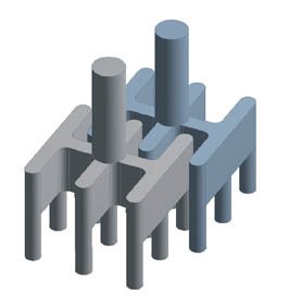
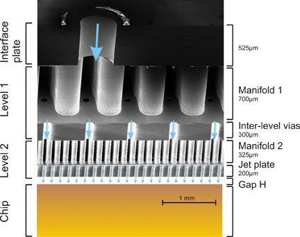
Looking beyond the limits of air-cooling systems, Zurich researchers are taking their concept of branched channel design even further and are developing a novel and promising approach for water-cooling. Called direct jet impingement, it squirts water onto the back of the chip and sucks it off again in a perfectly closed system using an array of up to 50,000 tiny nozzles and a complicated tree-like branched return architecture.
By developing a perfectly closed system, there is also no fear of coolant getting into the electronics on the chips. What's more, the IBM team was able to enhance the cooling capabilities of the system by devising ways to apply it directly to the back of the chip and thereby avoiding the resistive thermal interfaces in between the cooling system and the silicon.
First lab results are impressive. The team has demonstrated cooling power densities of up to 370 Watts per square centimeter with water as coolant. This is more than six times beyond the current limits of air-cooling techniques at about 75 Watts per square centimeter. Yet, the system uses much less energy for pumping than other cooling systems do.
