Increasing miniaturisation and spreading of functions became a global trend for the microelectronic industry. The system-in-package solution is of great importance for the realisation of highly integrated systems. SiP means that several different chips from different manufacturing technologies and structure widths are embedded side by side or stacked in one chip package and also function well. In the future, SiP components will be used in various fields of application, for example, in communication and computing technology, energy production and distribution, automotive electronics, medical equipment and LED-lightning.
With the help of ESiP new technologies are developed for chip integration in one SiP package and their production as well as reliability measurement processes and methods or devices for failure analysis and testing. Basic technologies have been developed for integration of different chips in the smallest of spaces in one SiP package. Not only the reliability of new production processes for SiP solutions with two or more different chips inside the case is to be investigated, but also the material required to build a SiP. For this purpose feasibility as well as reliability was an important factor in more than 20 breadboards.
As part of the ESiP project, processes and devices should be provided in order to analyze SiP components using heat flow thermography. For this, already existing processes and analysing devices of SiP components were used and adjusted. In addition, also new innovative failure analysis procedures, devices as well as software tools were created. The project focused on non-destructive detection of faults in electrical channels and determination of delamination at bond interfaces.
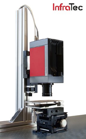
For this project, InfraTec developed a new high-definition thermographic camera module that uses the latest detector with currently the highest geometrical resolution of (1,280 x 1,024) IR pixels as well as the most sensitive thermal resolution of up to 0.02 K. Together with the newly developed microscope objective the system can achieve a geometrical resolution of approx. 2 µm. With those core components a lock-in-thermographic system has been established that supports different thermal stimulation types. Together with project partners, the established thermographic system has been successfully tested for different scenarios.
The ENIAC Joint Undertaking (JU) is a public-private partnership focusing on nanoelectronics that brings together ENIAC Member/Associated States, the European Commission, and AENEAS (an association representing European R&D actors in this field).

