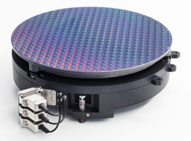
High-end microchips manufactured using 3 nm technology are the current state of the art. Production technologies for the 2 nm technology node are expected to be available as early as next year and for 1.4 nm, i.e., 14 angstroms, by 2027. The 95-million-euro research project 14ACMOS is co-funded by the European Union and supported by the “Joint Undertaking for Chips” (Chips JU). It brings together the know-how and development expertise of Europe's leading suppliers to the semiconductor industry. The project, which involves twenty-five partners from six countries, is coordinated by ASML, the Dutch world leader in lithography systems for semiconductor manufacturing.
PI has been a system partner to the semiconductor industry for decades and is represented worldwide with positioning systems in a wide range of areas of semiconductor production. In areas such as lithography and metrology for quality control, the nanopositioning specialist's products are already in use. The positioning systems to be developed as part of the 14ACMOS project must also function precisely and highly dynamically under vacuum conditions in order to be economically viable.
Link to the project: https://cordis.europa.eu/project/id/101096772
“This project is co-funded by the European Union under grant agreement No 101096772 and is supported by the Chips Joint Undertaking and its members.”
The angstrom scale is often used to describe atomic distances. One angstrom is equal to one ten millionth of a millimeter or 0.1 nanometers (nm). For comparison: A human hair is about 80,000 nanometers thick.

