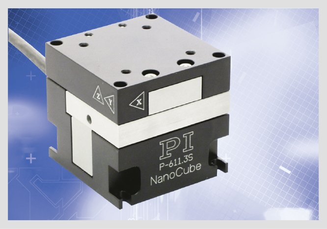
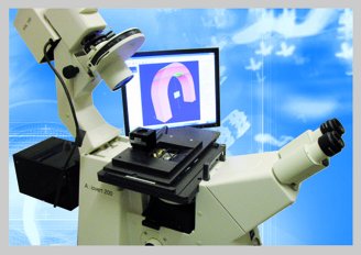
PI's range of highprecision stages - the NanoCube P-611 (Fig. 1) XYZ nanopositioning systems - prove their ability time and again in new fields of application. The cube sides measure a mere 44 mm, making it suitable for travel ranges up to 100 x 100 x 100 µm and easy to integrate. The stages are driven by piezo actuators and achieve resolutions of up to 0.2 nm at response times in the millisecond range. The basic (openloop) model is designed for highresolution positioning where the absolute position is of secondary importance or whose control loop is closed externally. This is the case with tracking or fiberpositioning applications, for example. A closedloop version with integrated position sensors is available for applications which require high accuracy both in absolute terms and also in terms of repeatability. Both versions use preloaded highperformance piezo actuators which are integrated into a frictionfree, zerobacklash guiding system with FEM optimized flexures. The actuators, guides and sensors are nonwearing, making the systems very reliable and durable. This has already been proven in numerous applications where high precision is required. One example can be found in a product from the French company Teem Photonics, which uses the NanoCube P-611 in the new µFab3D microfabrication system (Fig.2). The system builds threedimensional microstructures and objects in light sensitive materials such as polymers, proteins or noble metals.
The microfabrication system operates on the basis of socalled "twophoton absorption," where a pulsed beam of laser light is used to achieve a sufficiently high supply of energy at the focus. This changes the material structure by polymerization, cross linking of proteins or precipitations of metal ions. The typical fields of application include microfluidics, cell biology and the manufacture of photonic crystal structures in microoptics.
The resolution of the system, i.e. the size of the machining points, which can be anywhere within the object, is 200 nm. The objects are fabricated "on the fly" at a speed of 100 µm/s. For a homogenous and highquality result the laser must drive to the machining points precisely and with constant speed. The NanoCube P-611 provides the optimum conditions here with a travel range of 100 x 100 x 100 µm. Since the size of the object to be machined is currently limited solely by the travel range of the piezo system, a system with greater travel ranges will be used in the future.
Teem Photonics
Teem Photonics was founded in 1998 as a spinoff of Schneider Electronics. The company's headquarters are close to Grenoble in France. Products developed by Teem Photonics are used in a wide range of industrial and biophotonic applications. These include fluorescence spectroscopy and microdissection, for example. The products are marketed all over the world via branches and agencies in Europe, Asia, the Middle East, Canada and the USA. Teem Photonics USA in Massachusetts is a whollyowned subsidiary.


