Numerous industries are increasingly adopting laser processes for marking of products. The benefits are obvious: laser markings are waterproof and resistant to smudging, abrasion and solvents. Plus, they offer full design flexibility by not requiring stencils or solid moulds. The inherent contactless nature of laser processes makes marking and processing wear-free. And benefits accrue to other applications, too, such as durable direct bonding of electronic components on circuit boards.
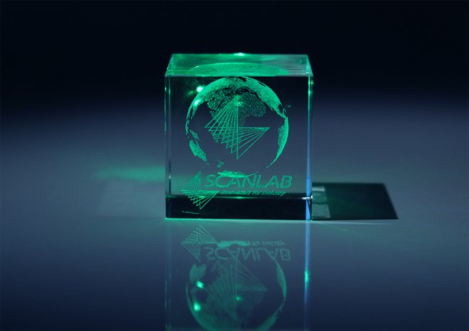
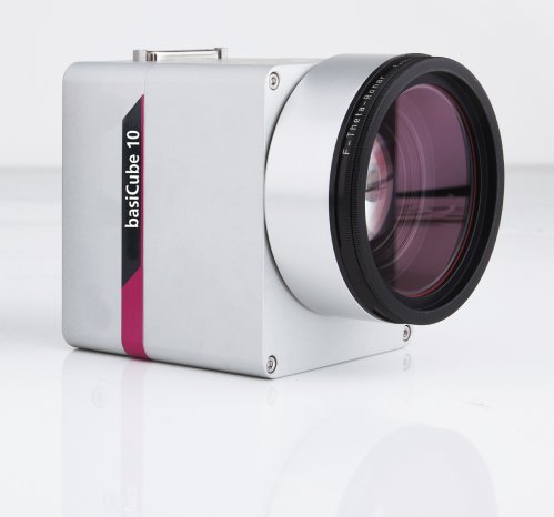
Introduced in early 2015, the compact, remarkably cost-effective and very fast basiCube scan head quickly met with market success. Now SCANLAB expands this product family with a variant specially optimized for green laser light applications at the 532 nm wavelength. Such lasers are particularly well-suited for processing of glass, silicon wafers and (precious) metals. They enable generation of even the finest contours by focusing to very small spot sizes while simultaneously maintaining excellent beam quality and low heat development. This allows engraving 3D shapes inside a glass body or welding copper wires directly onto the silicon substrates of integrated circuits. Application areas are virtually unlimited, ranging from medical products, decorative items or jewelry, all the way to the semiconductor industry.
Like SCANLAB's other scan systems, these new scan heads are manufactured in Germany to the highest quality standards. The system is exactly as energy-efficient as the other ‘family members’ – for equal writing performance, less electrical power is consumed compared to other systems. This characteristic also positively effects the system's positional stability under load.


