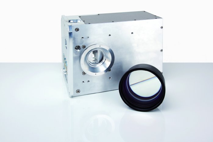
USP lasers are ideal for high-precision microprocessing of components. Cold ablation enables exceptionally fine and targeted material removal. But to achieve industry-suitable productivity, the USP laser must team up with an ultra-swift scanner capable of positioning the individual laser pulses onto a workpiece without pulse overlaps, even at highest pulse rates. In principle, the high speed of polygon scanners makes them well-suited for separating such high-frequency pulses. But pure polygon scanners have limitations in accuracy and flexibility and have been difficult to integrate into USP processing systems so far.
SCANLAB eliminated these drawbacks by developing a hybrid polygon scanner system combining the dynamic superiority of polygon scanners with the high precision of galvanometers. "Our many years of galvo expertise led to the idea of combining the systems. Two galvanometer scan axes now correct typical deviations and imperfections in polygon wheel symmetry to achieve the flexibility necessary for pixel-accurate processing," explains SCANLAB CEO Georg Hofner. "A large working distance, the straight-forward integration of the mechanical feed axis and incredibly short process times predestine this system for industrial applications."
Reduced Process Times - A Photovoltaic Example
The solar sector is under pressure to continuously lower costs for renewable power from photovoltaic systems. One possible response is the use of rear-contact cells to raise the efficiency of solar modules. SCANLAB, Innolas Systems GmbH and the Institute for Solar Energy Research Hameln (ISFH) jointly tested laser processing of crystalline Si solar cells, whereby the hybrid polygon scanner formed electrical busbars on the backs of cells - arranged as alternating strips of emitter and base regions. Here, the new scan system drastically reduced process times: full-surface back-side structuring of a 6-inch wafer previously required nearly a minute. SCANLAB's new polygon scanner cuts that process time to less than 5 seconds - with any pattern and at highest resolution.
This new technology is also suited for mobile devices, the electronics industry and the processing of composites. Hence, system development was supported by Germany's Federal Ministry of Economics and Energy. Test systems are now available from SCANLAB.


